Microelectronics and Nanotechnology Research Group
University of Manitoba - Department of Electrical and Computer Engineering


Characterization of active electrical traps in HfO2 high-κ dielectrics
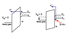
The continuous scaling of MOSFET has driven SiO2 gate dielectric to limits due to the exponential increase in gate leakage current with decreasing the gate oxide thickness. High-κ dielectrics have been used as the replacement to circumvent these problems. Many materials have been studied to replace SiO2 as the gate dielectric. Among these materials hafnium dioxide (HfO2) shows to be one of the more promising. Characterization of these materials in thin film form is important due to the dependence of macroscopic properties on microscopic structure. This project is concentrated on establishing the correlation between the electrical behavior of sputtered HfO2 high-κ dielectric thin films and its history which determines its physical structure.